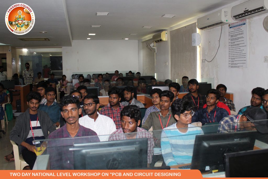
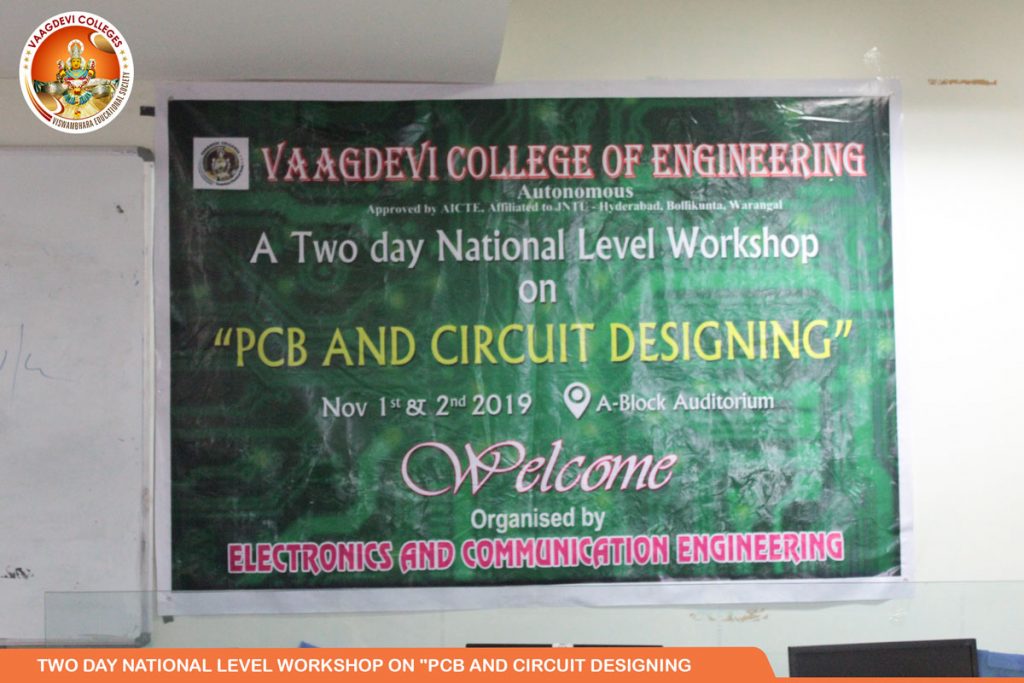
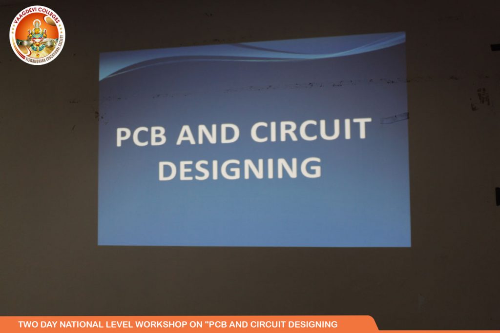
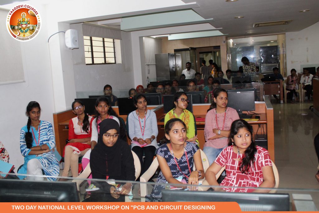
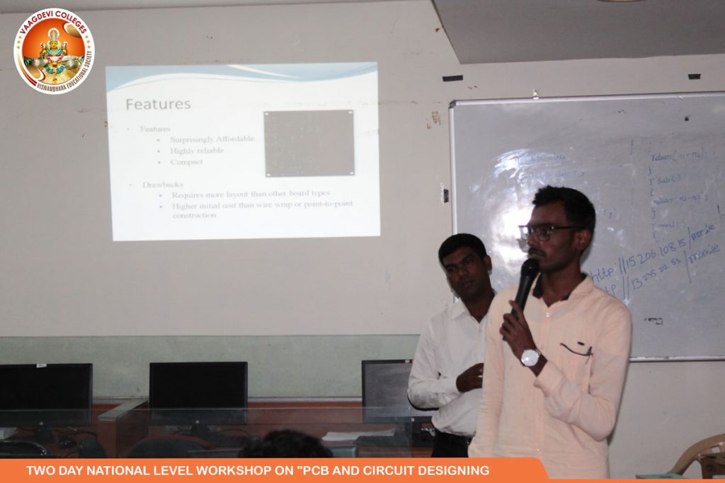
Students learn Schematic Design & Component Footprint Design in a Two Day National Level Workshop on “PCB and Circuit Designing” organised by Department of Electronics And Communication in association with Navica Communications Private Limited, inaugurated by Prof.K.Prakash, principal, VCEW in presence of Mr.M.Shashidar, Convenor, Dr.Jithesh Ramdas Shinde, HOD, ECE and coordinators, Ms.K.Swapna, Mr.U.Venu, Mr.Ch.AnilKumar
- Home
- About Us
- Academics
- College Academic Council
- Departments
- Academics
- Admissions
- Facilities
- Committees
- Board of Governors
- College Academic Council
- Finance Committee
- Board of Studies
- Grievance Redressal Committee
- Examinations and Result Processing Committee
- Planning and Evaluation Committee
- Admission Committee
- Library Committee
- Anti-Ragging Committee
- Internal Compliance Committee
- Purchase Committee
- Career Guidance Cell
- IQAC
- SC/ST-Cell
- RTI Cell
- EDC-Cell
- Institute Innovation Cell (IIC)
- III C
- Placements & Career Counselling Cell
- R&D Cell
- Extra-Curricular Activities Committee
- IPR Cell
- Placements
- For Employees
- Campus Life
